Loading...
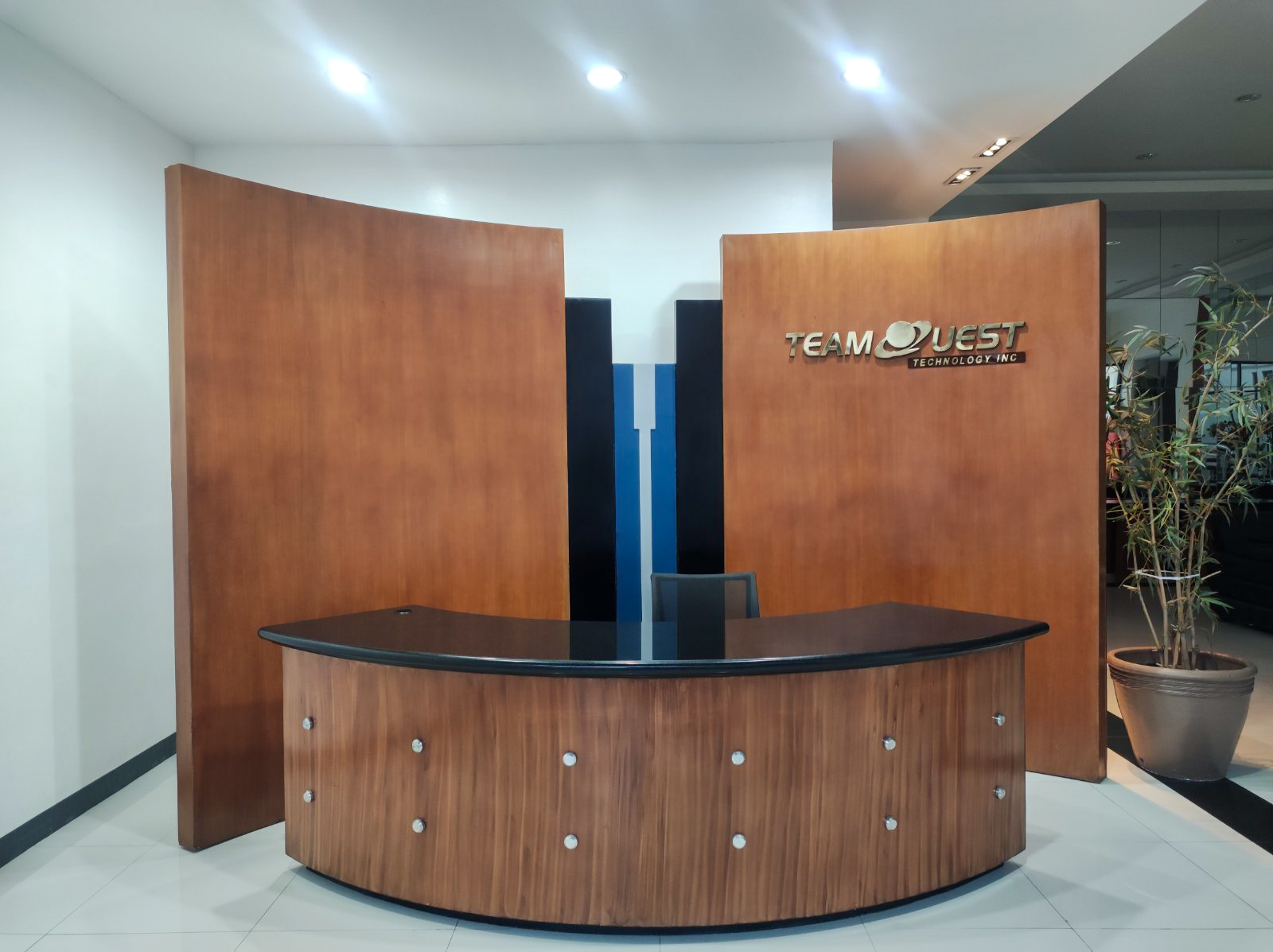
Welcome to TeamQuest
We are team of talented engineers with extensive experience on Semiconductor services
GET STARTEDAbout Us
Provide semiconductor services with 18 years of experience
Established in January 2006, TeamQuest Technology Inc., began as an inspection, sorting, and manpower service company for the semiconductor manufacturing sector in the Philippines.
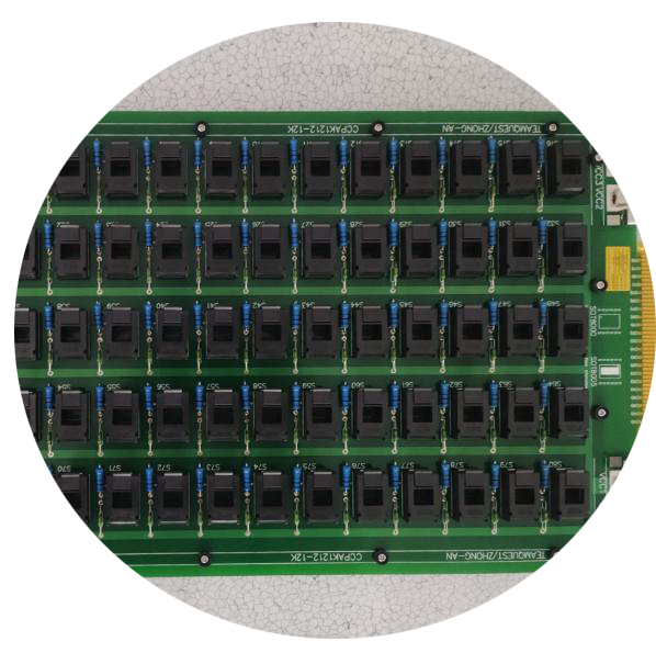
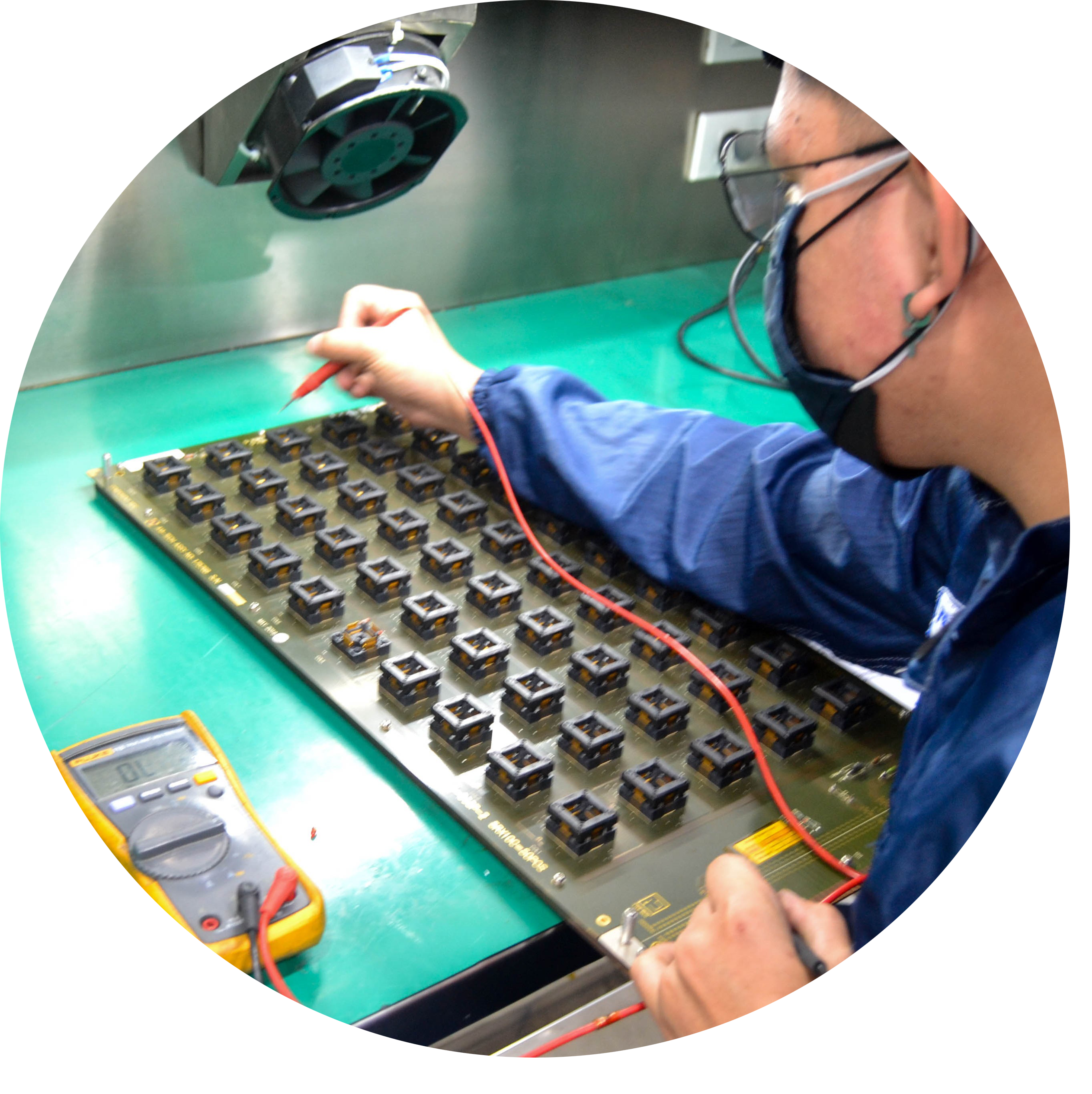
Over the years, we have expanded into a Testing facility that offers Semiconductor Burn-in services for production, reliability, and engineering. Additionally, we provide Turnkey burn-in boards and burn-in oven manufacturing, among related services.
Expert Engineering Team
Customer-Centric Approach
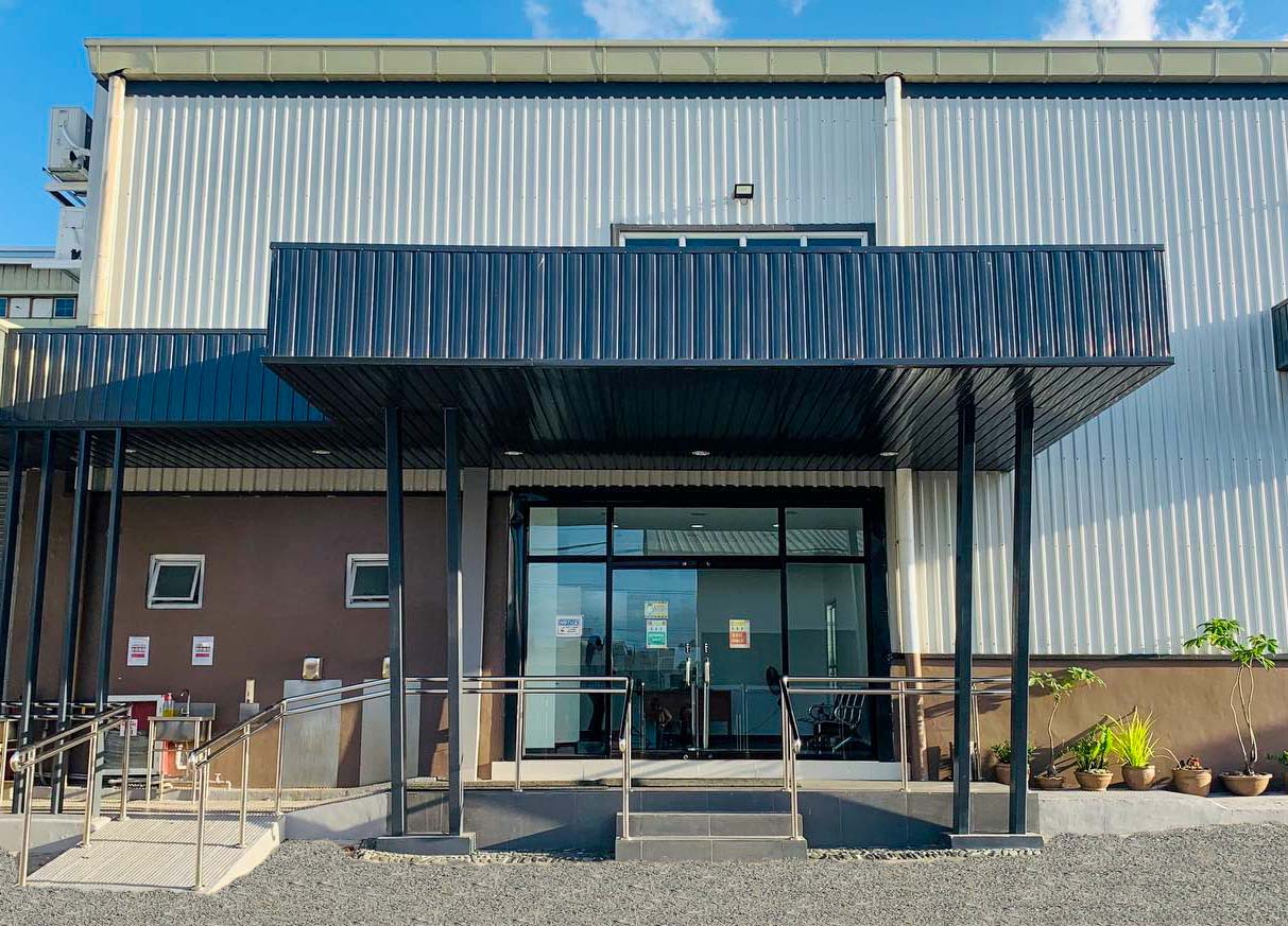
Adequate space and warehouse facilities
Global Collaborations
Proven Excellence
Compliance and Safety
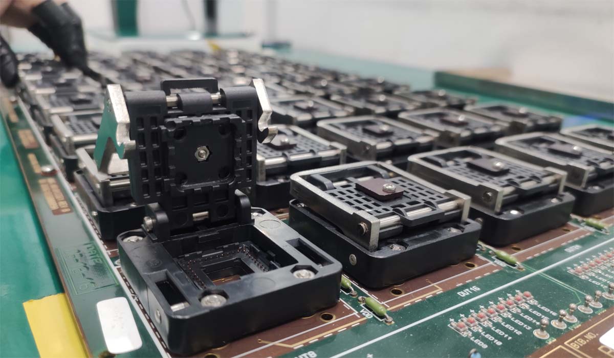
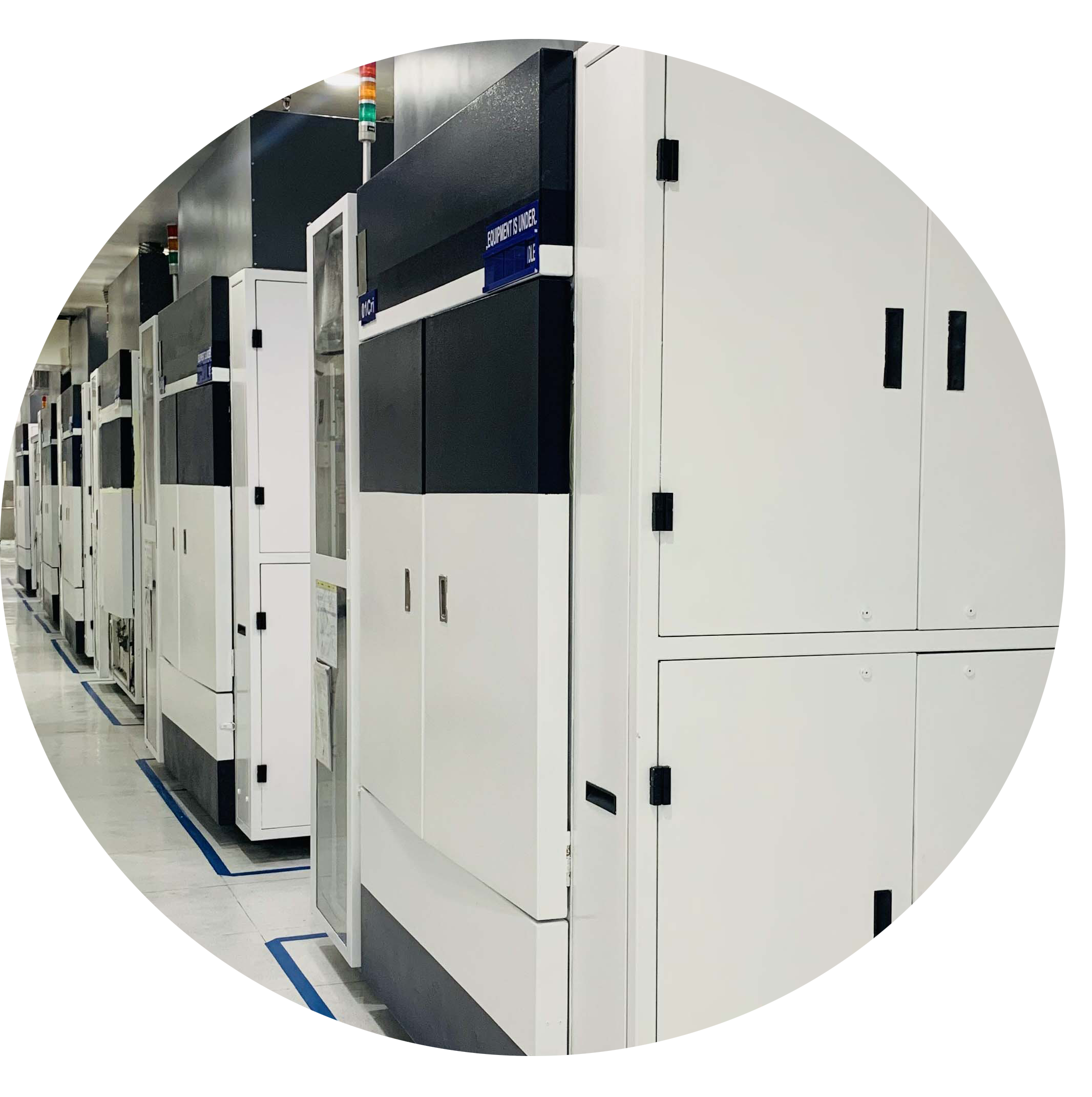
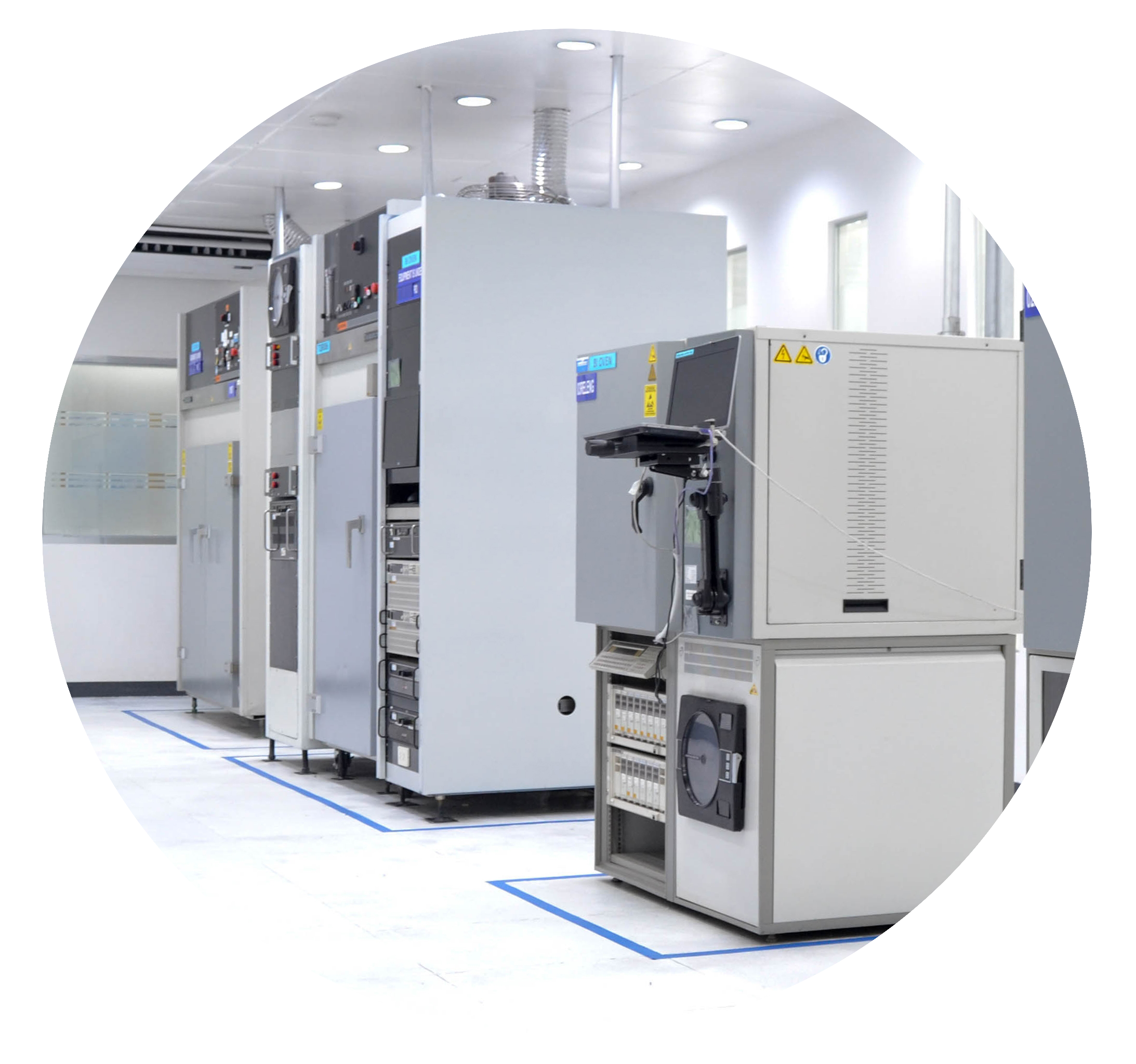
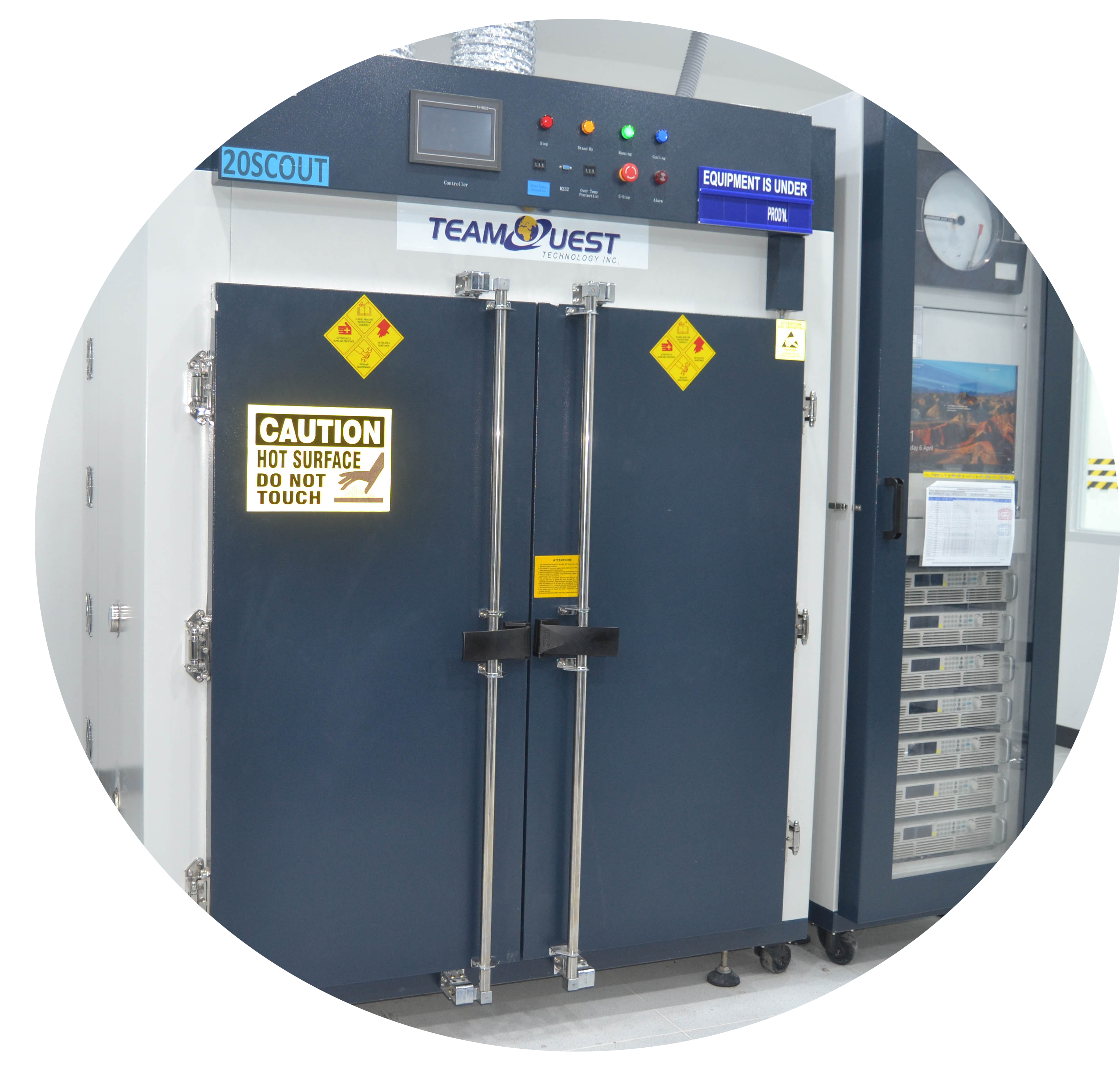
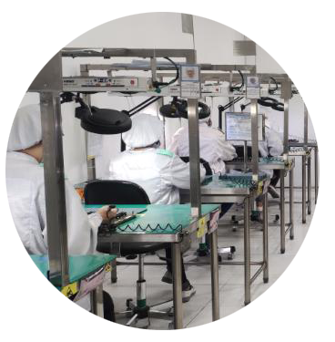
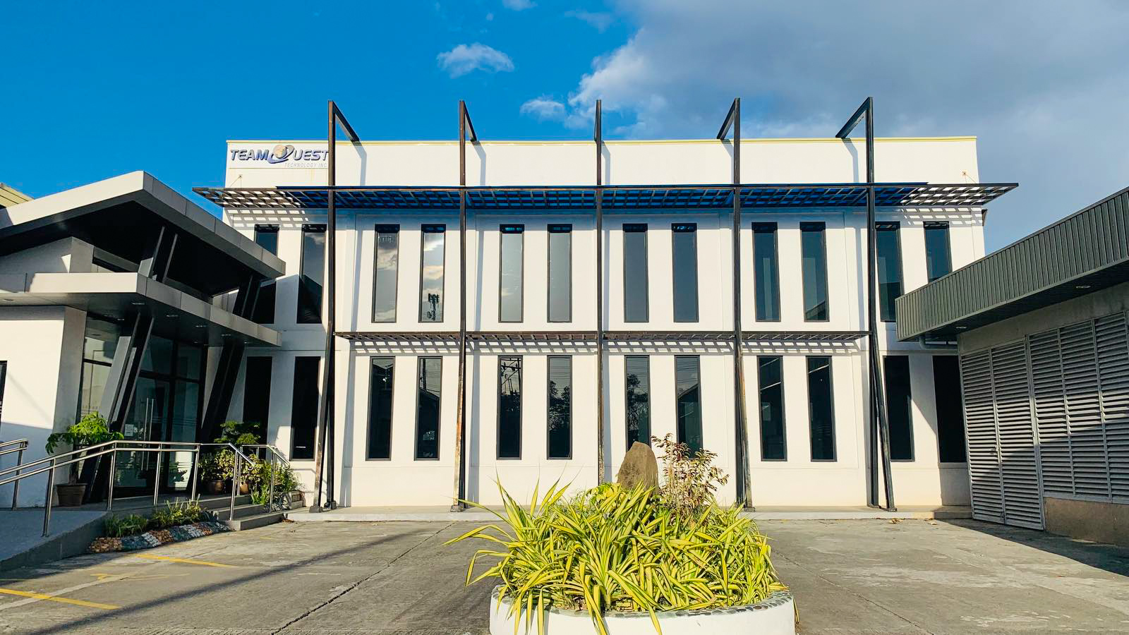
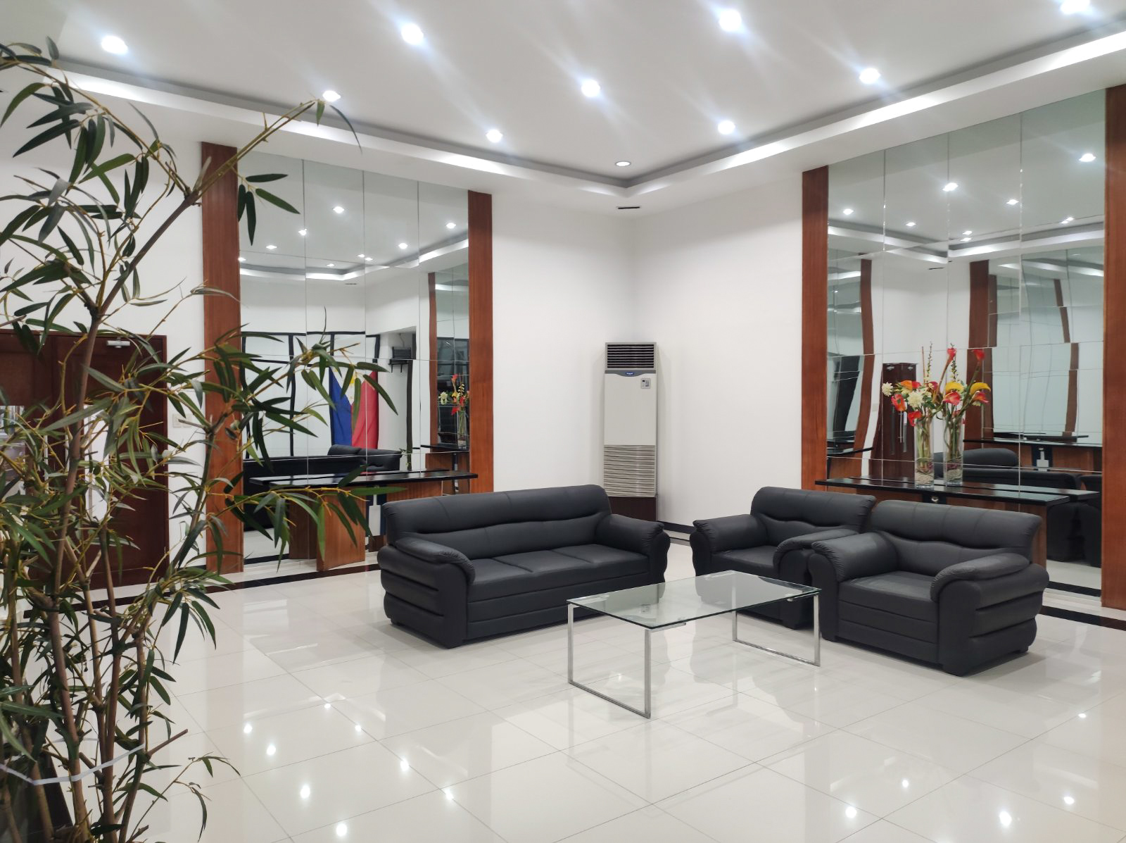
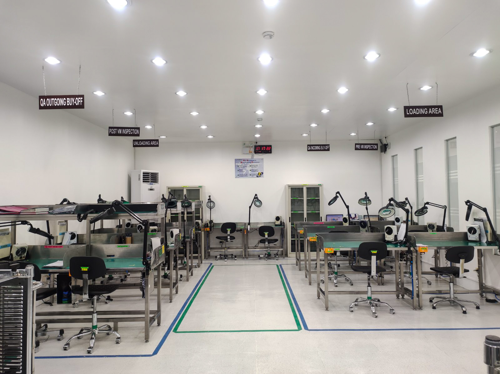
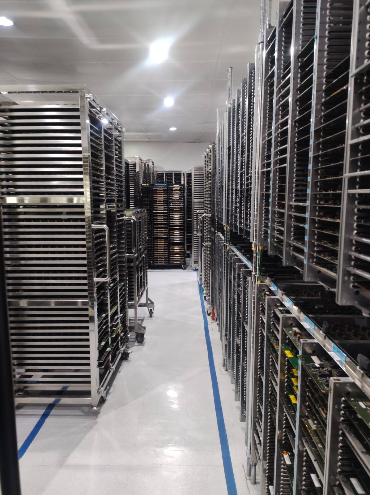
Our Facilities
Our facilities overview
- All
- Facilities
- Production